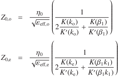
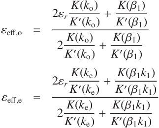
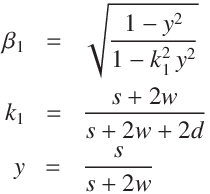
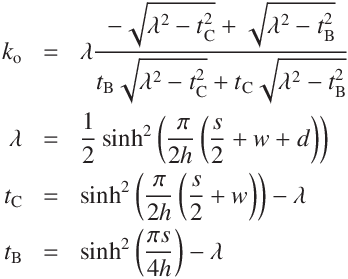
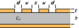
In this calculation, the ground planes are assumed to be wider than 6h + 2g + s + 2w and the conductor thickness is thinner than 0.35 w, and the upper conductor plane, if exists, is located higher than 15 (h + t).
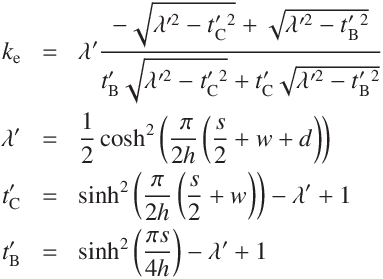
The above analytical solution by Hanna (1985) is for negligibly thin conductor thicknesses,
but the thickness of conductors used in real circuit boards has a non-negligible effect.
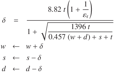
As I am unaware of any formula that includes conductor thickness,
I will use the following formula to compensate for the case where conductor thickness
t < 0.35w, 0.35s, 0.35d and the dielectric relative permittivity 2.2 < ϵr < 10.2.
This correction value of δ is not an analytical value,
but an approximate correction based on electromagnetic field simulations in the practical range,
so it may not be accurate enough in some cases.
However, as far as I have confirmed, it seems to be within ± 4 % of the impedance calculated by electromagnetic field simulation.
Without this correction, the error is more pronunced for large t / w, low relative permittivity and small gap.
e.g. t / w = 0.35, er = 2.2, s / w = 1, d / w = 1.5, the error is about 25 %.
The other simplest correction formula would be δ = t,
which yields a maximum error of 7 % when calculated under the same conditions.
Note: This formula is subject to change without notice due to experimental results for improvement.
REFERENCE
Victor Fouad Hanna, "Parameters of Couplanar Directional Couplers with Lower Ground Plane", 15h European Microwave Conference, 1985
Brian C. Wadell, "Transmission Line Design Handbook", Artech House, Inc., 1991, ISBN 0-89006-436-9
Rainee N. Simons, "Coplanar Waveguide Circuits, Components, and Systems", A JOHN WILEY & SONS, INC., 2001
David Kirkby, atlc — Arbitrary Transmission Line Calculator
APPENDIX 1
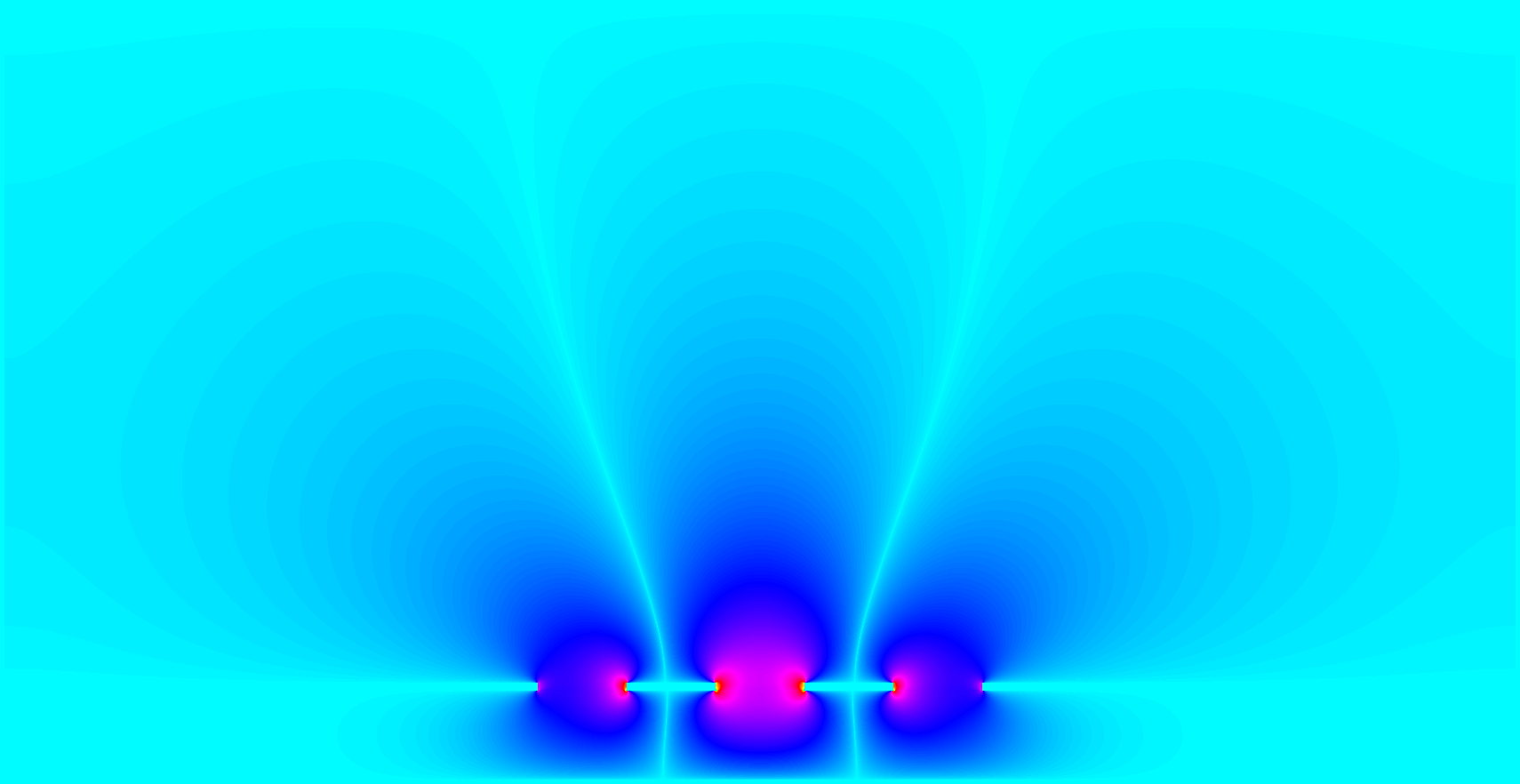
Examples of electromagnetic field simulations results (ground plane width b=3200, upper conductor height g=3200)
Length unit in [ μm ].
Pseudo color visualization of absolute value of the electric field in odd mode.
APPENDIX 2
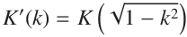
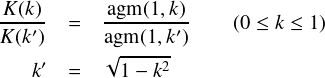
The ratio of the complete elliptic integrals of the first kind K(k) and K(k') can be calculated by the following relation with the ratio of arithmetic-geometric means (AGM).
The argument k is the elliptic modulus.
where agm(1, k) is the arithmetic-geometric mean of 1 and k.

![[Mail]](/~lyuka/images/mail.gif)


 © 2000 Takayuki HOSODA.