Rev.0.8 (Jan. 26, 2022)
Takayuki HOSODA
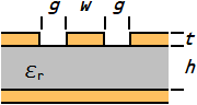
Calculate the characteristic impedance and effective dielectric constant of a conductor-backed coplanar waveguide.
OperationInput
Resources used
Output
Analyze Conductor-backed Coplanar Waveguide. Rev.0.8 (Jan. 26, 2022)
(c) 2022 Takayuki HOSODA00 { 205-Byte Prgm } 01>LBL "K" ; Complete elliptic integral of the first kind K(k) 02 X↑2 03 1 04 X<>Y 05 - 06 SQRT 07>LBL "K'" ; K(k') | compensation modulus k' = √(1 - k2) 08 1 09>LBL 00 10 ENTER 11 ENTER 12 RCL× ST T 13 SQRT 14 R↓ 15 R↓ 16 + 17 0.5 18 × 19 R↑ 20 X=Y? 21 GTO 01 22 R↓ 23 GTO 00 24>LBL 01 25 R↓ 26 + 27 PI 28 X<>Y 29 ÷ 30 RTN 31>LBL "cbcpw" 32 MVAR "er" 33 MVAR "h" 34 MVAR "w" 35 MVAR "g" 36 MVAR "t" 37 VARMENU "cbcpw" 38 STOP 39 EXITALL 40 RCL "t" 41 0 42 X≥Y? 43 GTO 02 44 X<>Y 45>LBL 02 46 ENTER ; Conductor thickness compensation Δ 47 RCL+ "w" ; w + Δ 48 PI 49 4 50 RCL× "h" 51 ÷ 52 RCL "g" 53 R↑ 54 - ; g - Δ 55 ENTER 56 + 57 R↑ 58 + 59 R↑ 60 RCL÷ ST Y 61 STO 00 62 R↑ 63 RCL× ST T 64 TANH 65 R↑ 66 RCL× ST T 67 TANH 68 ÷ 69 STO 01 70 XEQ "K'" 71 STO 03 72 RCL 00 73 XEQ "K'" 74 STO 02 75 RCL 01 76 XEQ "K" 77 STO 01 78 RCL 00 79 XEQ "K" 80 STO 00 81 RCL 02 82 RCL× 01 83 RCL 00 84 RCL× 03 85 ÷ 86 ENTER 87 RCL× "er" 88 1 89 + 90 X<>Y 91 1 92 + 93 ÷ 94 ENTER ; Effective permittivity εeff 95 SQRT 96 RCL 00 97 RCL÷ 02 98 RCL 01 99 RCL÷ 03 100 + 101 × 102 188.365156834 ; Characteristic impedance of free space η0 / 2 103 X<>Y 104 ÷ 105 RTN ; Characteristic impedance of the CBCPW Z0 106 END
Download : cbcpw.raw (raw program file for Free42)
Input Output
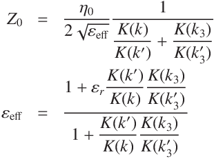
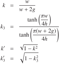
where
η0 is the intrinsic impedance of vacuum ≈ 376.730313 Ω
and K(k) is the complete elliptic integral of the first kind.

![[Mail]](/~lyuka/images/mail.gif)


 © 2000 Takayuki HOSODA.