Noise calculation in Op.Amp circuit

waveform

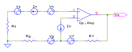
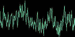
Figure 1. Noise model
simplified schematic

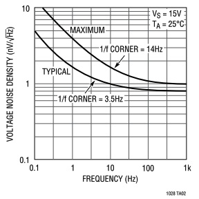
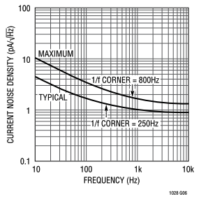
Figure 2. Example of noise spectrum of an actual Op.Amp
Voltage noise densityVoltage noise density
(LT1028/LT1128 datasheet Rev.C, 1992, p1-p6)
Rs : Source resistance    Ω
Rg : Gain resistor    Ω
Rf : Feedback resistor    Ω
Ta : Absolute temparature    K
Vn : Input refered voltage noise density of the Op.Amp.   V/√Hz
In : Input refered current noise density of the Op.Amp.    A/√Hz
fv : 1/f voltage noise corner frequency of the Op.Amp.    Hz
fb : 1/f current noise corner frequency of the Op.Amp.    Hz
fh : Higher frequency  (Bandwidth = fh - fl)  Hz
fl : Lower frequency    Hz
Vr : Jhonson noise of the source resistance Rs at Ta  V/√Hz
Vd : Input refered voltage noise density of the amplifier at flat region.  V/√Hz
En : Input refered voltage noise of the amplifier over the bandwidth.  Vrms
Eo : Output voltage noise of the amplifier over the bandwidth.  Vrms
peak-to-peak (limits of 99.7% of the time; 6×RMS)  Vp-p
Noise power into 50 Ohm  dBm
"Noise calculation in Op.Amp circuit Rev.1.02 (Mar. 7, 2015)", Finetune co., ltd.

APPENDIX

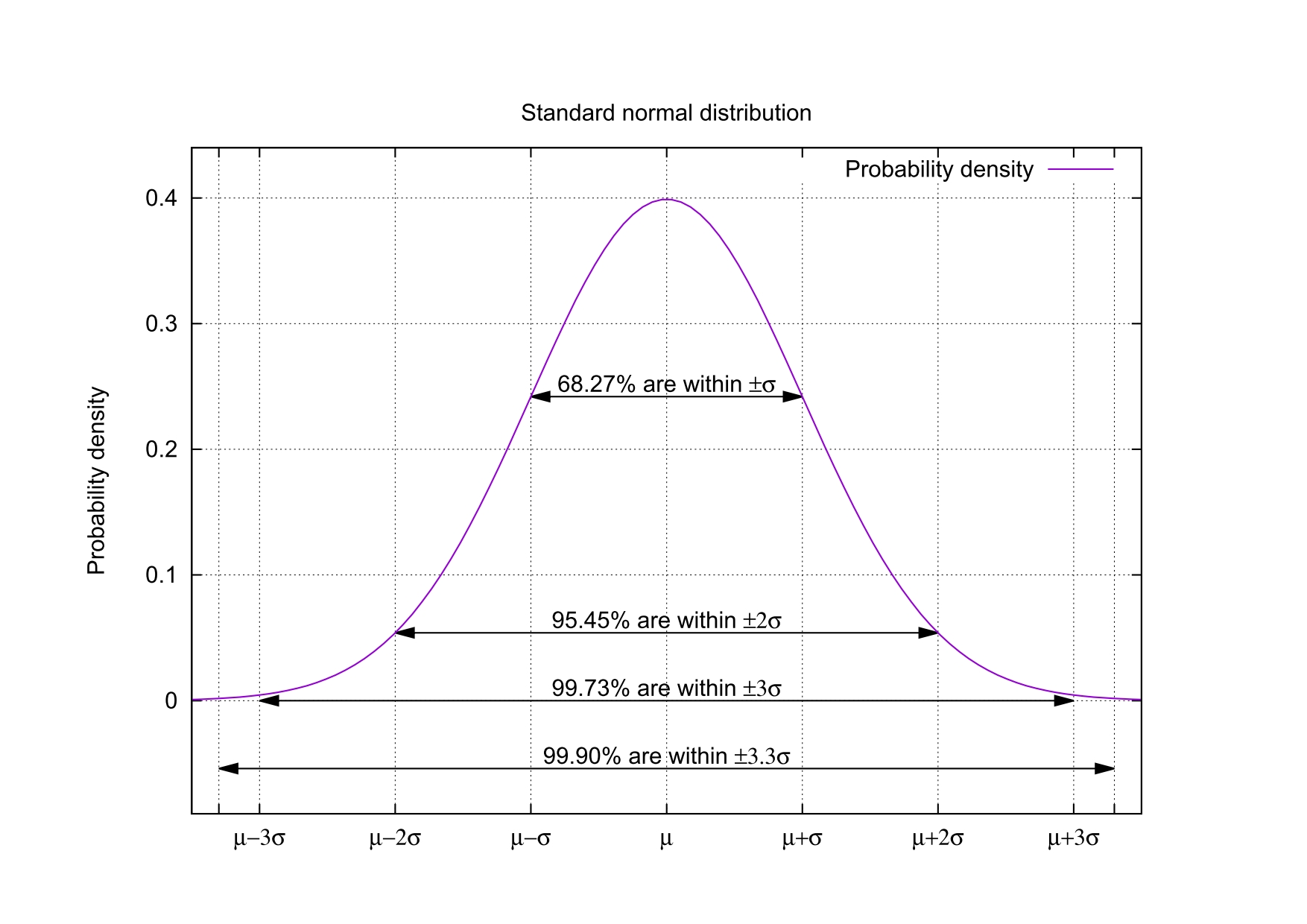
Figure 3. Standard normal distribution
standard normal distribution

REFERENCE

"Noise Calculation in Op Amp Circuits - Design Note 15", Linear Technology Corporation, 1988
"LT1028/LT1128 - Ultralow Noise Precision High Speed Op Amps", Linear Technology Corporation, 1992

SEE ALSO

vn - noise culculation program for the HP 42s

www.finetune.co.jp [Mail] © 2000 Takayuki HOSODA.